Ofer Adan
MSc Graduate - 2002


 ++ 972 52 872 437

Current occupation: R&D Physicist and a senior applications development
engineer at a semiconductor industry leader of process diagnostics and control.
Inventor of patent in electron optics engineering, and an
active publishing author on semiconductor process diagnostics and control
topics.
 The
research (Sep 99 – April 02 ):
The
research (Sep 99 – April 02 ):
(Co-supervision of
Prof. Zohar Yosibash with
Prof. Roni Schneck from
Material Eng Dept.)
Thermo-Elastic
Failure Investigation of Electronic Components, using Stress Check - Funded
project:
The objectives of
Ofer Adan’s study were to investigate and prevent
thermo-mechanical failures occurring in microelectronic VLSI devices during the
manufacturing process. A mismatch of the elastic constants and thermal
expansion coefficients between aluminum interconnects and Si3N4
passivation layers causes initiation of 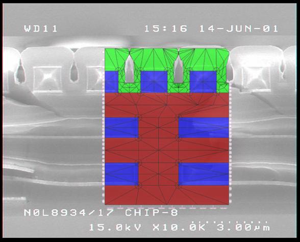 mechanical failure in
passivation layers. This is due to thermo elastic loading while cooling of the
devices from the passivation deposition chamber. Cracks initiate at re-entrant
corners, the dimensions of which are of micron size, and propagate into the
interconnect layers, where they may be detrimental to the device operation.
mechanical failure in
passivation layers. This is due to thermo elastic loading while cooling of the
devices from the passivation deposition chamber. Cracks initiate at re-entrant
corners, the dimensions of which are of micron size, and propagate into the
interconnect layers, where they may be detrimental to the device operation.
A criterion for
failure initiation at a tip-notch is proposed, based on the elastic strain
energy density (SED) in the vicinity of the tip-notch; A
multilevel parametric model of such a device (according to manufacturer’s
nomenclature) has been prepared and the stresses and SED had been found by the
finite element method (FEM). A promising conformance between crack locations
and the location of maximum tangential stresses at the tip of the passivation
notches (Key-hole geometries due to nonconformal step
coverage of the passivation over neighboring aluminum line interconnects) has
been found. Validation of the model was necessary in order to enable the
determination by calculation of the critical SED providing a quantitative
failure criterion with applicability for a variety of situations. Thus an
experiment has been designed and accomplished to find the failure envelope by
full-scale wafer production at extreme fabrication conditions. The results
enable us to correlate and determine the (SED)cr failure criterion so to predict and prevent
failures in the manufacturing process of VLSI structures.